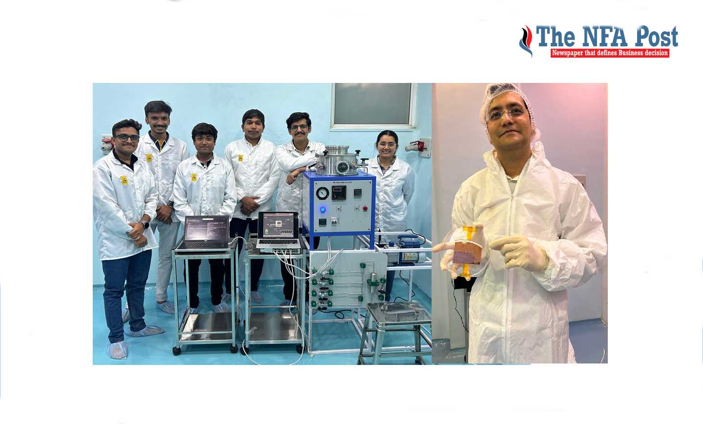
Led by Marmik Bhatt, a seasoned expert with around decade of experience in chip fabrication, home-grown Monk9 Tech’s model showcases how startups can create cost-effective, market-ready chips for applications like IoT and analog chips.
Bengaluru, NFAPost: India’s semiconductor industry is witnessing local innovation driven transformation, creating unhindered opportunities for startups and small to medium enterprises (SMEs) to innovate in chip design and manufacturing.
At the forefront of this movement is Monk9 Tech, a Rajkot, Gujarat-based company pioneering a low-volume semiconductor fabrication facility (fab) that produces chips at 130nm to 350nm nodes. This article explores how Monk9 is making chip production accessible and affordable, enabling smaller players to compete in the global semiconductor market.
Led by Marmik Bhatt, a seasoned expert with nearly a decade of experience in chip fabrication, Monk9 Tech is redefining the semiconductor landscape in India. By leveraging open-source tools, refurbished equipment, and local expertise, the company has developed a cost-effective model that eliminates the need for massive capital investments typically associated with chip manufacturing.
This approach allows startups and SMEs to produce market-ready chips for applications such as Internet of Things (IoT) devices and analog chips, which are in high demand across industries like automotive and consumer electronics.
Monk9’s journey began with a vision to democratize chip production. Bhatt, who previously represented ChipIgnite for Efabless.com in India, the Middle East, and Southeast Asia, recognized the potential of open-source tools and process design kits (PDKs) to lower entry barriers for small companies.
Starting with a baseline product at 350nm, Monk9 focused on moderately complex chips like 8-bit microcontrollers (MCUs) and analog-to-digital converters (ADCs). The company’s reliance on open-source software, developed by Indian scientists, has enabled it to create chips without costly electronic design automation (EDA) tools, making the process both affordable and scalable.
The company’s innovative “lab-to-fab” approach further sets it apart. Initially, Monk9 validated its processes in nanoscience labs, including those at Indian Institutes of Technology (IITs) and private facilities, before establishing its own fab.
By salvaging academic equipment and optimizing processes, Monk9 ensures repeatability and cost efficiency, distinguishing its fab from traditional lab setups. The company has also navigated infrastructure challenges with support from the Gujarat government and local industry partners, building a robust ecosystem for semiconductor production.
Monk9’s efforts align with India’s broader push to become a global semiconductor hub, bolstered by initiatives like the India Semiconductor Mission and the Gujarat Semiconductor Policy. These policies, combined with a growing supply chain, are fostering an environment where startups can thrive. Monk9’s focus on legacy nodes like 130nm and 180nm, which account for a significant portion of the global market, caters to local demand for applications in IoT and automotive sectors, reducing reliance on foreign manufacturers.
By providing open-source EDA tools and affordable tape-out services, Monk9 is empowering small businesses to innovate without the financial burden of licensing fees or high-end equipment. This model not only drives technological advancement but also positions India as a leader in accessible semiconductor innovation.
As Monk9 continues to scale its operations, its story serves as a blueprint for how Indian startups can carve a niche in the global chip-making ecosystem, fostering entrepreneurial growth and technological self-reliance.

Editor, EEHerald