
Designed and taped out in Bengaluru, Qualcomm’s 2-nanometer chip signals India’s arrival as an end-to-end semiconductor powerhouse—and tightens the link between chip sovereignty and the country’s AI ambitions.
Bengaluru, NFAPost: India’s long journey from being the world’s technology back office to becoming a serious force in deep-tech innovation has reached a defining milestone. Qualcomm’s successful 2-nanometer (2nm) chip tape-out, executed with substantial engineering ownership in India, is not merely a technical achievement—it is a strategic inflection point for the country’s semiconductor and AI roadmap.
At a time when only a handful of global companies and nations can operate at such advanced nodes, the announcement underscores a decisive shift: India is no longer just contributing labour to global silicon programs; it is co-creating the future of advanced computing.
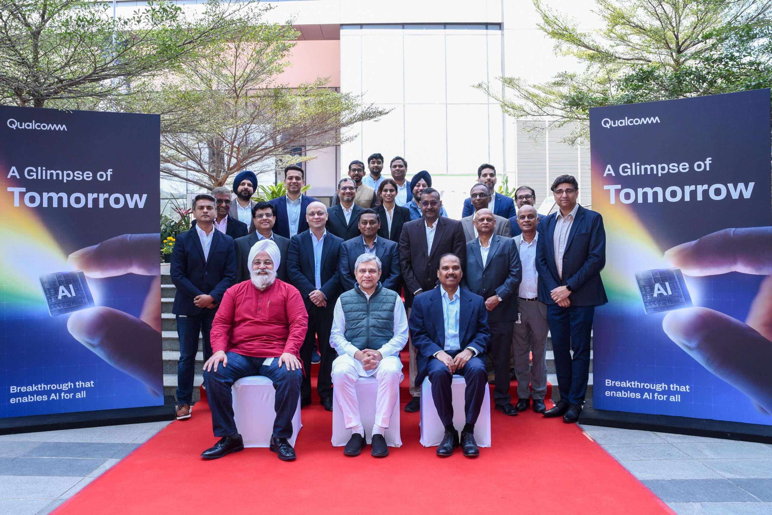
Unveiled at Qualcomm’s Bengaluru facility during a high-level government visit, the 2nm design represents one of the most complex semiconductor efforts undertaken in India to date. Each die integrates 20–30 billion transistors, combining CPU and GPU capabilities optimised for next-generation AI workloads, edge computing, and intelligent connected systems.
“Today we unveiled the two-nanometer wafer and two-nanometer chip at Qualcomm,” a senior executive said during the briefing.
“Each die carries close to 30 billion transistors. This enables an AI computer—not just in the cloud, but on the edge: inside cameras, Wi-Fi routers, vehicles, industrial machines, even aircraft.”
Beyond Engineering Support: Full Silicon Ownership
The true significance of this milestone lies less in transistor density and more in process ownership. Qualcomm confirmed that Indian teams are now deeply involved across the entire silicon lifecycle—from customer product definition and architecture, to physical design, tape-out, and validation.
“Gone are the days when India was doing only back-office development work,” one official noted.
“Today, the journey—from customer requirement to validated silicon—is happening here.”
This evolution reflects a broader industry pattern. Global semiconductor firms such as AMD have also expanded India’s role from execution to architecture and product leadership. The result is the emergence of a self-sustaining design ecosystem, rather than isolated centres of excellence.
Talent: The Engine Behind the Silicon Push
Such complexity would be impossible without a deep talent base—and this is where India’s Semiconductor Mission has quietly rewritten expectations. Initially conceived to train 85,000 semiconductor engineers over ten years, the programme has already produced around 67,000 trained professionals in just four years.
More than 315 universities and colleges across the country are now equipped with advanced EDA tools, enabling students to design chips and, in some cases, tape out real silicon at the Mohali semiconductor laboratory.
“What India has built in such a short time is exceptional,” said a senior policymaker.
“Students are not just learning theory—they are designing, validating, and taping out chips.”
This model has drawn international attention. At Davos, global semiconductor leaders openly acknowledged that India is uniquely positioned to address a looming global talent gap estimated at nearly one million professionals over the next decade.
Semicon 2.0: A Deliberate, Long-Horizon Strategy
Building on early momentum, the government has outlined Semicon 2.0, a roadmap that prioritises design leadership as the foundation of semiconductor sovereignty. Manufacturing scale, equipment, materials, and advanced packaging follow in carefully sequenced stages.
India’s current fabrication capability begins at 28nm. The next milestones are ambitious but measured: 7nm within the coming years, followed by a gradual progression toward 3nm and 2nm nodes later in the decade.
“Semiconductor manufacturing is not a sprint; it is a multi-decade marathon,” an official said.
“We are consciously learning to walk before we run—studying the paths taken by Japan, South Korea, and Taiwan.”
This realism marks a departure from headline-driven policymaking and reflects a deeper understanding of the capital intensity, yield learning curves, and ecosystem depth required to succeed in advanced fabrication.
AI, Data Centres, and the Compute Imperative
The semiconductor push is inseparable from India’s AI ambitions. Under the national AI mission, India has already deployed 38,000 GPUs in shared compute infrastructure, with another 20,000 GPUs slated for near-term addition.
This surge is driving a parallel boom in data centres. Committed investments currently stand at $70 billion, with announced figures touching $90 billion. Officials expect total investments to cross $200 billion as hyperscalers, enterprises, and sovereign compute initiatives scale up.
“Data centres will be one of the biggest growth engines in the coming years,” a senior official said.
“And wherever data centres go, manufacturing ecosystems follow.”
That prediction is already materialising. Two companies are preparing announcements for AI server manufacturing facilities in India, supported by local PCB and electronics manufacturing—early signs of a vertically integrated hardware ecosystem.
Qualcomm’s India Bet: A Two-Decade Payoff
For Qualcomm, this milestone is the culmination of more than 20 years of sustained investment in India. Today, its engineering centres in Bengaluru, Hyderabad, and Chennai form one of the company’s largest and most advanced R&D footprints outside the United States, spanning wireless, compute, AI, and system-level engineering Press Release_Qualcomm Reinforc….
Union Minister Ashwini Vaishnaw, who visited the Bengaluru campus during the showcase, framed the achievement in strategic terms:
“India is increasingly at the centre of how advanced semiconductor technologies are being designed for the future,” he said.
“Seeing Qualcomm’s engineering depth and long-term commitment here strongly aligns with our vision of a globally competitive semiconductor industry.”
Senior Qualcomm leaders echoed this view, emphasising that India is now integral—not auxiliary—to the company’s global engineering roadmap.
“Working on advanced nodes like 2nm demands the very best talent,” a Qualcomm executive said.
“Our India teams consistently deliver at a global standard.”
A Structural Shift, Not a Symbolic One
With the next phase of the AI Mission set to be finalised after a summit of over 100 global AI leaders, and Semicon 2.0 nearing formal rollout under the India Semiconductor Mission, India’s technology strategy is entering a phase of execution at scale.
The 2nm tape-out in Bengaluru is not an endpoint. It is evidence of a structural shift—from cost-led participation to capability-led leadership. For a country seeking both digital sovereignty and global relevance in AI, advanced silicon may prove to be the most strategic foundation of all.


Leave a Reply