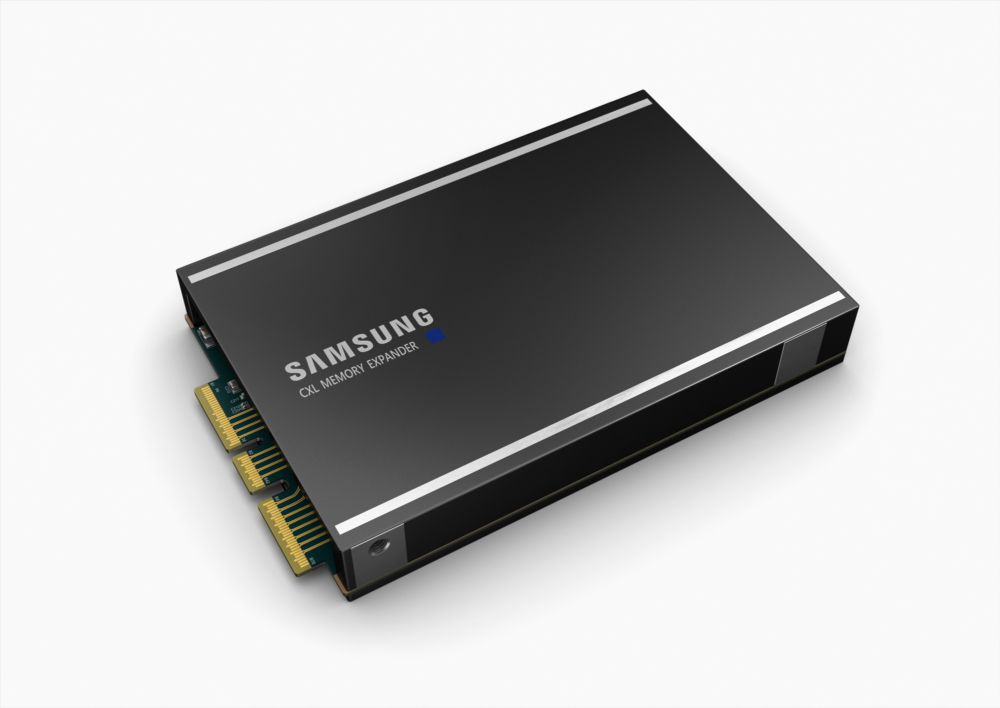
DDR5 DRAM-based memory module is designed to meet the high-performance demands of data-intensive applications including AI and HPC
CXL interface enables memory capacity to scale to the terabyte level and substantially reduces system latency
Samsung Electronics, the world leader in advanced memory technology, today unveiled the industry’s first memory module supporting the new Compute Express Link (CXL) interconnect standard.
Integrated with Samsung’s Double Data Rate 5 (DDR5) technology, this CXL-based module will enable server systems to significantly scale memory capacity and bandwidth, accelerating artificial intelligence (AI) and high-performance computing (HPC) workloads in data centers.
The rise of AI and big data has been fueling the trend toward heterogeneous computing, where multiple processors work in parallel to process massive volumes of data.
PCI Express
CXL—an open, industry-supported interconnect based on the PCI Express (PCIe) 5.0 interface—enables high-speed, low latency communication between the host processor and devices such as accelerators, memory buffers and smart I/O devices, while expanding memory capacity and bandwidth well beyond what is possible today.
Samsung has been collaborating with several data center, server and chipset manufacturers to develop next-generation interface technology since the CXL consortium was formed in 2019.
DRAM-based memory
Samsung Electronics Vice President Memory Product Planning Team Cheolmin Park said this is the industry’s first DRAM-based memory solution that runs on the CXL interface, which will play a critical role in serving data-intensive applications including AI and machine learning in data centers as well as cloud environments.
“Samsung will continue to raise the bar with memory interface innovation and capacity scaling to help our customers, and the industry at-large, better manage the demands of larger, more complex, real-time workloads that are key to AI and the data centers of tomorrow,” said Cheolmin Park.
Debendra Das Sharma, Intel Fellow and Director of I/O Technology and Standards at Intel, said Data center architecture is rapidly evolving to support the growing demand and workloads for AI and ML, and CXL memory is expected to expand the use of memory to a new level.
Memory ecosystem
“We continue to work with industry companies such as Samsung to develop a robust memory ecosystem around CXL,” highlighted Debendra Das Sharma.
Dan McNamara, senior vice president and general manager, Server Business Unit, AMD, added that AMD is committed to driving the next generation of performance in cloud and enterprise computing.
“Memory research is a critical piece to unlocking this performance, and we are excited to work with Samsung to deliver advanced interconnect technology to our data center customers,” said Dan McNamara.
CXL hardware
Unlike conventional DDR-based memory, which has limited memory channels, Samsung’s CXL-enabled DDR5 module can scale memory capacity to the terabyte level, while dramatically reducing system latency caused by memory caching.
In addition to CXL hardware innovation, Samsung has incorporated several controller and software technologies like memory mapping, interface converting and error management, which will allow CPUs or GPUs to recognize the CXL-based memory and utilize it as the main memory.
Samsung’s new module has been successfully validated on next-generation server platforms from Intel, signaling the beginning of an era for high-bandwidth, low latency CXL-based memory using the latest DDR5 standard.
The Korean technology conglomerate is also working with data center and cloud providers around the world to better accommodate the need for greater memory capacity that will be essential in handling big data applications including in-memory database systems.
As the DDR5-based CXL memory module becomes commercialized, Samsung intends to lead the industry in meeting the demand for next-generation high-performance computing technologies that rely on expanded memory capacity and bandwidth.
Chip Packaging Technology
Samsung Electronics has developed an advanced chip packaging technology for high-performance applications as the South Korean tech giant eyes to expand its leadership in semiconductor solutions.
The company said its next-generation 2.5D packaging technology, Interposer-Cube4 (I-Cube4), is expected to be widely used in areas like high-performance computing, artificial intelligence (AI), 5G, cloud and largest data center applicants as it creates enhanced communication and power efficiency between logic and memory chips.
I-Cube is Samsung’s brand for its heterogeneous integration technology that horizontally places one or more logic dies, such as central processing units (CPU) and graphics processing units (GPU), and several high bandwidth memory (HBM) dies on a paper-thin silicon interposer and makes them operate as a single chip in one package.
Mold-free structure
Samsung said it used a unique mold-free structure for the I-Cube 4 solution, which incorporates four HBMs with one logic die, for better thermal management and stable power supply, reports Yonhap news agency. The company added it also improved its yield with its prescreening tests and reduced the number of process steps to save costs and cut turnaround time.
Samsung said it will try to incorporate more chips in one package as the company is researching how to deal with interposer warpage and thermal expansion through changes to material and thickness.


